Car Specification Silicon Carbide Power Module - Substrate and Epitaxy Chapter
The latest data from the China Association of Automobile Manufacturers shows that from January to November 2022, the production and sales of new energy vehicles reached 6.253 million and 6.067 million respectively, a year-on-year increase of twice, and the market share reached 25%. It can be seen that the development of new energy vehicles has entered the fast lane. Here we note that due to mileage anxiety and fast charging requirements, the 800V battery bus system has gained the favor of many OEMs or Tier1. When it comes to the 800V bus system, let's focus on the core power device, silicon carbide power module. Due to the unique advantages of silicon carbide, it is very suitable for manufacturing high voltage, high junction temperature, and high-speed MOSFETs. These three heights precisely meet the requirements of the 800V bus system for core power devices. Ansemi is very optimistic about the development of 800V busbar systems, and some research institutions predict that by 2026, SiC will account for over 12% of the entire power device market.
Ansemy has been involved in the field of silicon carbide for a long time, starting the research and development of SiC devices as early as 2004. However, Ansemy has been fully investing in the silicon carbide field since its acquisition of GT Advanced Technologies (GTAT) in 2021, in terms of funding, human and material resources, as well as customers and markets. After acquiring GTAT, Ansemy began its vertically integrated supply chain in the silicon carbide field - from crystals to systems! Next, we will analyze and introduce the key supply chain substrates and epitaxial EPI of two silicon carbide, so that everyone can have a further understanding of Ansemy's layout and leading advantages in silicon carbide.
Ansemy Silicon Carbide Fully Vertically Integrated Supply Chain - From Crystal to System
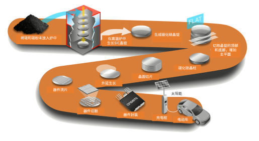
The supply chain starts with the growth of single crystal SiC powder materials at our factory in Hudson, New Hampshire. A thin epitaxial layer is grown on the substrate, followed by multiple complex device processing steps to produce the chip, which is then packaged into the final product. The entire manufacturing process is vertically integrated end-to-end, with comprehensive reliability, traceability, and comprehensive quality testing to ensure zero defect requirements for products.
The fully vertically integrated supply chain has considerable advantages in the current supply chain system, such as easy expansion of production capacity, excellent quality, and cost control. Especially in the current supply chain of silicon carbide, every link is not so easy to reliably produce high-quality products, which is different from the silicon supply system. In the supply chain of silicon, silicon wafers (substrates) are usually handed over to third parties for production, and the quality, cost, and yield of the third party are quite good. Next, we will proceed with the production of substrates and epitaxial layers, so that everyone can understand why Ansemy has chosen a fully vertically integrated supply chain model in the silicon carbide field. This has also made Ansemy one of the few companies in the world with capabilities ranging from substrate to module to system.
Crystal/Substrate
Our chips are made by adding a thin epitaxial layer on top of the substrate before being used to make the chip. How is the substrate produced and manufactured? There are two steps involved here. Firstly, the silicon carbide powder is placed in a long crystal furnace to grow into crystals and obtain silicon carbide ingots. The silicon carbide ingots need to be polished, then sent for cutting and polished to obtain the wafer substrate required for our device production. Figure 1 is a schematic diagram and physical photo of a long crystal furnace.
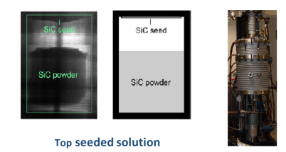
Figure 1 Schematic diagram and physical object of the long crystal furnace
This involves two key steps, crystal growth, ingot cutting, and polishing. Figure 2 is a schematic diagram of our production process from silicon carbide powder to substrate
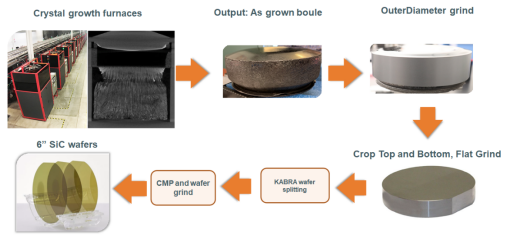
Figure 2 Production Flow Chart of Silicon Carbide Substrate
At present, the most mature methods for growing silicon carbide crystals are PVT and CVD, both of which belong to meteorological phase growth, while the silicon carbide forms are mainly 4H and 6H.
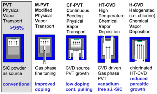
Figure 3: Growth mode of silicon carbide crystal
Firstly, let's take a look at the challenges faced by crystal growth
·To have high-quality seed crystals (seeds)
·Techniques for reducing crystal defects from seed crystals to newly grown crystals
·Crystal growth requires high temperature (>2000 ° C)
At these temperatures and growth times, few materials remain inert and are prone to reactions.
·Polymorphism - Up to 220 types, currently available mainly with 4H and 6H
·Inconsistent decomposition (gas: Si, Si2C, SiC), (solid: carbon)
·Purity at Source - Nucleus Points of Defects
·Compared to Si, the aspect ratio of ingots is often lower
·The main challenge facing the entire industry is to grow longer defect free crystals
·Enlargement of crystal diameter (currently at a maximum of 8 ")
O No cracks, high crystal quality (grain boundaries, defects, etc. near the edge of the wafer)
GTAT itself started from producing and manufacturing long crystal furnaces, and now has about 20 years of experience in the design and manufacturing of silicon carbide long crystal furnaces. For these challenges of crystal growth, GTAT has rich experience. We have high-quality seed crystals, good temperature control, and excellent defect control technology, as well as excellent defect detection and identification capabilities.
When it comes to defects in silicon carbide, the following are several typical defects in silicon carbide crystals
·Crystal instability
·Open core dislocation (microtubule)
·Closed nuclear screw dislocation
·Low angle grain boundaries
·Conventional dislocation
·Basal plane dislocation (BPD) - basal plane edge dislocation or partial BPD
·Thread edge misalignment (TED)
·Overlay fault/conversion
These defects are all generated during the substrate or ingot stage, but once they are generated, they cannot be eliminated. They will continue to propagate to the epitaxial layer, ultimately affecting the quality of the device. So we not only need to identify them in the substrate stage, but also in the epitaxial layer to exclude them. This poses a challenge to the external extension layer.
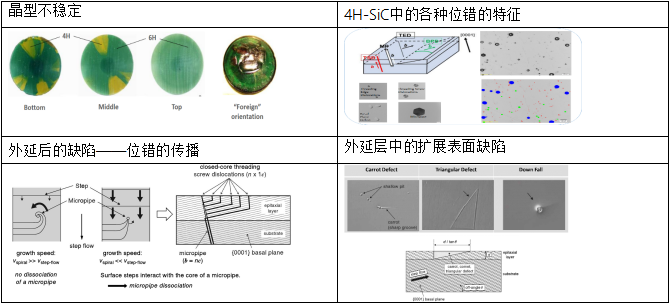
Figure 4 Defects in Silicon Carbide Substrate
High quality crystals are the cornerstone of the entire silicon carbide supply chain, and GTAT has accumulated considerable production experience in these areas, ensuring that Ansemy's silicon carbide devices are completed on a high-quality substrate. At the same time, we can also expand production very quickly, which is also an aspect of Ansemy's competitiveness.
Epitaxy - EPI Epitaxy
The silicon carbide epitaxial layer refers to the part of the silicon carbide device manufacturing process that grows and deposits on the wafer substrate. Why do we need extension? In some cases, it is necessary for silicon carbide to have a very pure surface with the same crystal structure as the substrate, and to maintain control over the type and concentration of impurities. This is achieved by depositing an epitaxial layer on the surface of a silicon carbide substrate. In power devices, almost every unit of our device is processed in the epitaxial layer, and the importance of its quality for the device is evident. Different devices have different requirements for epitaxy. The deviation and defect requirements of diodes for epitaxy and the requirements of MOSFETs for them are two different levels of requirements. MOSFETs have high requirements for epitaxial quality. The deviation of doping will affect the distribution of Rdson in MOSFETs. Some defects can cause MOSFETs to have high leakage current, and in severe cases, they can lead to MOSFET failure.
Currently, the relatively mature processing technology for epitaxy is CVD, which has led many people to mistakenly believe that epitaxy is relatively easy to process. In fact, this is a misconception. Epitaxy is not simply about buying back the CVD furnace to make them good. Of course, compared to crystal substrates, it is relatively simple, but it does not mean it is easy to do well. The challenges faced by epitaxy and crystal substrates are different. Many people also say that many companies in the market now have the ability to process the epitaxial growth of diodes. They only need to upgrade their equipment a little to grow the epitaxial growth of MOSFETs very well. This statement needs to be discussed. Because as mentioned in the article, MOSFETs and diodes have different requirements for epitaxy, and their requirements for consistency and warpage are not on the same order of magnitude. In the epitaxial aspect, Ansemy also has rich experience. Prior to the acquisition of GTAT, Ansemy had over 10 years of experience in the epitaxial and wafer production research and development of silicon carbide. Therefore, we will continue to maintain this advantage by expanding both substrate production and epitaxial production.
Compared to ingot substrates, the challenges of epitaxy mainly focus on the following indicators:
·Thickness and consistency
·Doping and consistency
·Rapid detection and identification tracking capabilities for surface defects
·Rapid detection and identification tracking capabilities for bottom defects
·Control extension defects
·Cleaning
·Control of Warpage of Large Size Wafers
Let's categorize the detected defects.
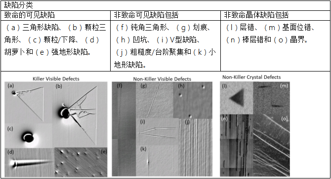
Figure 5 Epitaxial Defects
The following figure shows a complete MOSFET active cell, which includes defects in the substrate and then derived from epitaxial defects.
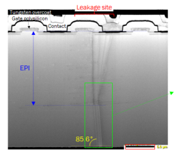
Figure 6: Defect Profile of Silicon Carbide MOSFET - Substrate Epitaxial Defects
To summarize, since the defects of the substrate cannot be eliminated in the epitaxial layer, we will adopt certain strategies to worsen the fatal defects, and then screen them out. This requires the substrate defects to be traceable in the epitaxial process, so companies that produce both the substrate and epitaxial layers themselves have a natural advantage. It can effectively control the defect rate.
Due to the limited correlation between substrate and epitaxial technology and chip development, I will share these two processes separately with you. The following chip technology developments, such as the planar or groove structures of MOSFETs, are directly processed in the epitaxial layer. Therefore, we can discuss the future technological development separately. Ansemy vertically integrates its internal resources on both the substrate and extension of the supply chain, so for customers, their supply is predictable. This is why many global customers have actively signed long-term supply agreements with Ansemy because our supply model provides them with long-term protection.
